
T0980
Preliminary Information
Rev. A4, 08-Dec-00
1 (7)
SiGe Transmit / Receive Front End IC
Description
The T0980 is a monolithic SiGe transmit/ receive front
end IC with power amplifier & low noise amplifier.
Electrostatic sensitive device.
Observe precautions for handling.
Features
D High power added efficient power amplifier
(Pout typ. 29 dBm)
D Controlled output power
D Low noise preamplifier (NF typ. 1.7 dB)
D Few external components
D PSSO16 plastic package with down set paddle
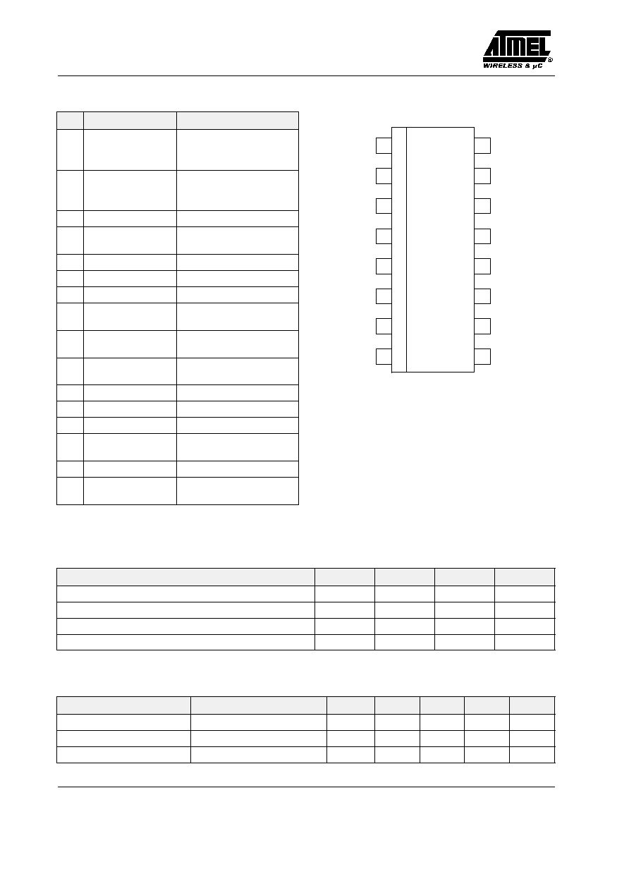
Block Diagram
Bias
16
13
11
9
1
3
5
8
Figure 1. Block diagram
Ordering Information
Extended Type Number
Package
Remarks
T0980-TJS
PSSO16
Tube
T0980-TJQ
PSSO16
Taped and reeled
T0980
Rev. A4, 08-Dec-00
Preliminary Information
2 (7)
Pin Description
Pin
Symbol
Function
1
V2_PA_OUT
Inductor to power supply
and matching network for
power amplifier output
2
V2_PA_OUT
Inductor to power supply
and matching network for
power amplifier output
3
GND
Ground
4
POUT_CONTROL
Power amplifier control
input
5
GND
Ground
6
LNA_IN
Low noise amplifier input
7
GND
Ground
8
BIAS_LNA
Resistor to Vs sets the
LNA current
9
VS_CTRL
Supply voltage for con-
trol of power amplifier
10
LNA_OUT
Low noise amplifier out-
put and supply voltage
11
GND
Ground
12
PA_IN
Power amplifier input
13
GND
Ground
14
V1_PA
Supply voltage for power
amplifier
15
GND
Ground
16
V2_PA_OUT
Matching network for
power amplifier output
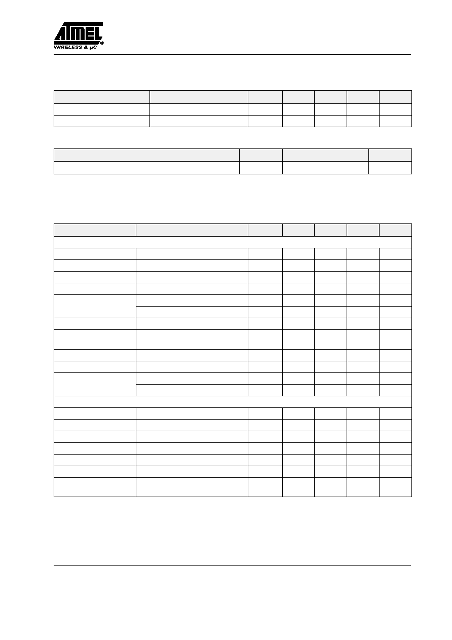
1
2
3
4
5
6
7
8
16
15
14
13
12
11
10
9
GND
POUT_
CONTROL
GND
LNA_IN
GND
BIAS_LNA
V2_PA_OUT
V2_PA_OUT
V1_PA
GND
PA_IN
GND
LNA_OUT
VS_CTRL
V2_PA_OUT
GND
T0980
Figure 2. Pinning PSSO16
Absolute Maximum Ratings
All voltages are referred to GND
Parameter
Symbol
Min.
Max.
Unit
Supply voltage PA, TX
Pins 1, 2, 9 and 14
Vs_PA
4.5
V
Supply voltage LNA, RX
Pin 10
Vs_LNA
2.8
V
Junction temperature
Tjmax
150
_C
Storage temperature
Tstg
�55
+125
_C
Operating Range
All voltages are referred to GND. The following table represents the sum of all supply currents.
Parameter
Test Conditions / Pins
Symbol
Min.
Typ.
Max.
Unit
Supply voltage PA
TX,
Pins 1, 2, 9 and 14
Vs_PA
3.6
4.4
V
Supply voltage LNA
RX,
Pin 10
Vs_LNA
2.5
2.6
V
Supply current PA
TX,
Pins 1, 2, 9 and 14
Is_PA
400
mA
T0980
Preliminary Information
Rev. A4, 08-Dec-00
3 (7)
Operating Range (continued)
All voltages are referred to GND. The following table represents the sum of all supply currents.
Unit
Max.
Typ.
Min.
Symbol
Test Conditions / Pins
Parameter
Supply current LNA
Pins 10 and 8
Is_LNA
2.5
mA
Ambient temperature
Tamb
�25
25
60
_C
Thermal Resistance
Parameter
Symbol
Value
Unit
Junction ambient
R
thJA
25
K/W
ESD Protection: t.b.d.
Electrical Characteristics
Test conditions (unless otherwise specified) : Vs_PA = 3.6 V, Tamb = 25
�
C.
Parameter
Test Conditions / Pins
Symbol
Min.
Typ.
Max.
Unit
Power amplifier
1)
Supply voltage
TX, Pins 1, 2, 9 and 14
Vs_PA
3.6
V
Supply current
TX, Pins 1, 2, 9 and 14
Is_PA
400
mA
Frequency range
TX
f
400
500
MHz
Power gain
TX
Gp
33
dB
Control voltage
TX, output power (max), Pin 4
2.5
V
g
TX, output power (min), Pin 4
0.7
V
Control current
Pin 4
0
400
�
A
Shut-down mode
Control voltage
0.1 V,
Pins 1, 2, 9 and 14
Is_PA
10
�
A
Power added efficiency
TX @ 450 MHz
PAE
50
%
Saturated output power
TX, input power 3 dBm
Psat
29
dBm
Harmonics
TX, input power 3 dBm
2 fo
�20
dBc
TX, input power 3 dBm
3 fo
�20
dBc
Low-noise amplifier
Supply voltage
RX, Pins 8 and 10
Vs_LNA
2.5
V
Supply current
RX @ R1 = 5.6 k
W, Pins 8 and 10 Is_LNA
2.5
mA
Frequency range
RX
f
400
500
MHz
Power gain
RX @ R1 = 5.6k
W, Is=2.5 mA
Gp
19
dB
Noise figure
RX @ R1 = 5.6 k
W, Is=2.5 mA
NF
1.7
2.5
dB
Isolation
RX @ R1 = 5.6 k
W, Is=2.5 mA
ISO
20
dB
3rd-order input inter-
ception point
RX @ R1 = 5.6 k
W, Is=2.5 mA
IIP3
�10
dBm
Notes : 1)
Power amplifier shall be unconditional stable, maximum duty cycle 100%, true cw-operation,
maximum load mismatch 10:1 for 5 s @ 3.6 V

T0980
Rev. A4, 08-Dec-00
Preliminary Information
4 (7)
Typical Characteristics
�20
�10
0
10
20
30
40
50
60
70
�50
�40
�30
�20
�10
0
10
20
P
AE ( % )
Pin ( dBm )
Gain
PAE
Pout
Gain ( dB )
Pout ( dBm )
Figure 3. Power sweep
0
10
20
30
40
50
60
70
0.0
0.5
1.0
1.5
2.0
2.5
3.0
3.5
P
AE ( % )
Vramp ( V )
PAE
Pout
Pout ( dBm )
Figure 4. Ramp sweep
0
10
20
30
40
50
60
70
0
1
2
3
4
5
P
AE ( % )
VCC ( V )
PAE
Pout
Pout ( dBm )
Figure 5. VCC sweep

T0980
Preliminary Information
Rev. A4, 08-Dec-00
5 (7)
Application Circuit T0980 (460 MHz)
1
Bias
2
3
4
5
6
7
8
10
11
12
13
14
15
16
9
L4
6.8nH
C8
2.7pF
C1
1nF
C3
100pF
R3
39
L2
39nH
L5
22nH
L6
4.7nH
L1
1.5nH
C10
12pF
C11
100pF
PA_OUT
C9
100pF
POUT_CTRL
LNA_IN
BIAS_LNA
C13
100pF
R1
5.6k
C14
8.2pF
C16
NC
L7
22nH
PA_IN
LNA_OUT
C4
NC
C5
3.9pF
L3
22nH
C6
100pF
C18
10nF
R2
0
VS_CTRL
C7
100pF
C17
NC
VS_PA
C15
100pF
GND
C2
1uF
C12
1uF
VS_LNA
T0980
Figure 6. Typical application circuit T0980 (460 MHz)